W.A.F.E.R.
Si Wafer?
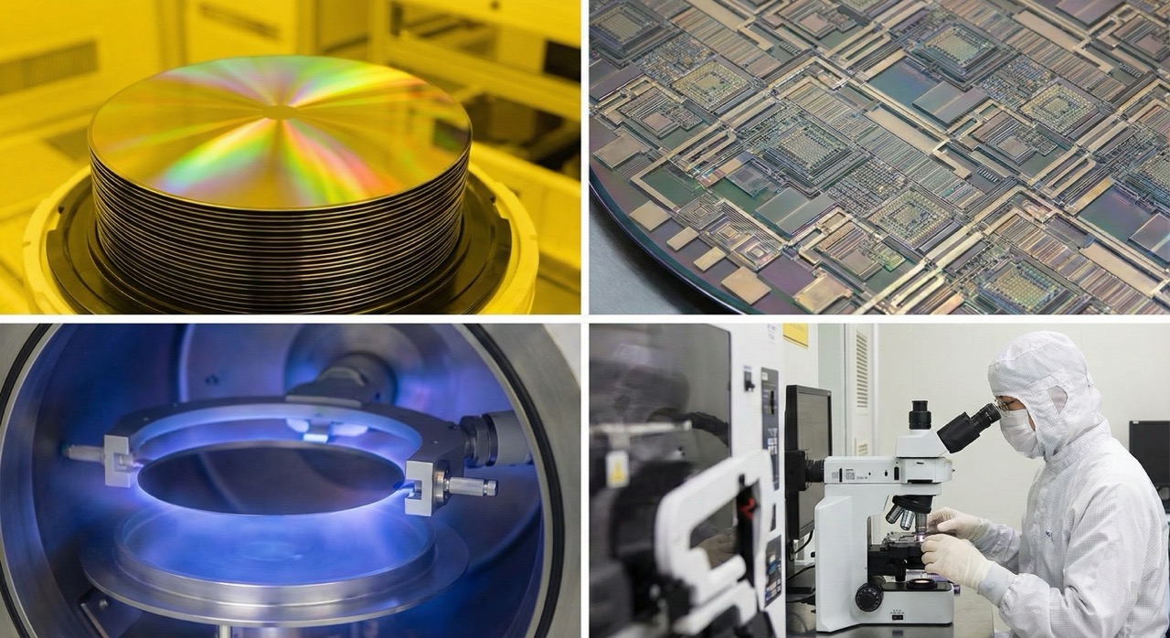
Silicon Wafer (Silicon Wafer), which is widely used as a material for semiconductor devices, is a single-crystal silicon thin plate made from polycrystalline silicon (Si) as a raw material.
Silicon exists in nature in the form of oxides (SiO2) in sand, stones, and minerals, and is a very abundant element that accounts for about 1/3 of the Earth's crust. Due to this abundance, non-toxicity, and stability, it is evaluated as an environmentally excellent material for the semiconductor industry.
Wafers made of silicon have a wide energy band gap (Energy Band gap, 1.2eV), allowing devices to operate at relatively high temperatures (about 200°C).
Silicon is extracted from sand, refined into high-purity polycrystalline silicon, and then single-crystal silicon wafers are manufactured. Using these wafers, various devices such as DRAM, ASIC, TR, MOSFET, CMOS, PMOS, ROM, and EP-ROM are manufactured, and these devices are currently used as core components in all industrial fields, including electronic products, industrial automation equipment, computers, and satellites.
As semiconductor devices become highly integrated, device yield and quality tend to respond sensitively to the characteristics of the wafer, which is the raw material.
Wafer quality characteristics (crystal defects) such as COP, FPD, OISF, and LDP (theoretically existing) appear sequentially from the center to the edge of the wafer, and it has been confirmed that this affects device yield and quality.
To solve these problems, a new concept of defect-free silicon (SD, Defect-Free Silicon) wafer has been developed that completely removes crystal defects and greatly improves quality uniformity from the center to the edge of the wafer.